Research/Publications
Md Yekra Rahman, Sharif Mohammad Mominuzzaman. “Exploring Lead Free Mixed Halide Double Perovskites Solar Cell,” 2024 13th International Conference on Electrical and Computer Engineering (ICECE), Dhaka, Bangladesh, 2024, pp. 165-170, doi: 10.1109/ICECE64886.2024.11024609.
Projects
DC-DC Buck Converter
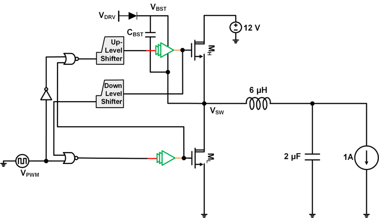
- Designed a synchronous buck converter (12 V → 3.3 V, 1 A, 2 MHz) using the TSMC 180 nm Technology in Cadence Virtuoso.
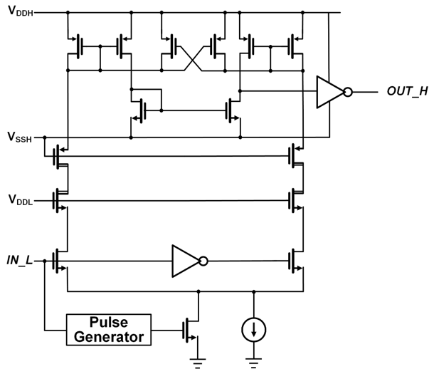
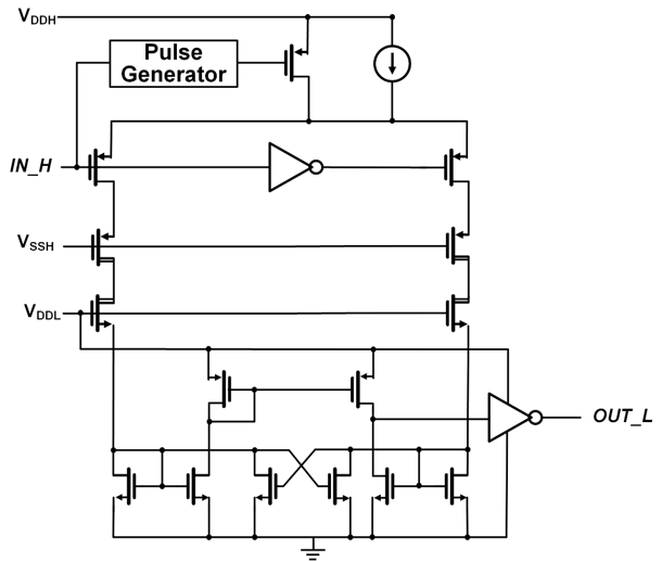
- Optimized high-/low-side MOSFET dimensions through efficiency sweeps; developed a custom gate driver with level shifters, bootstrap, and dead-time control to minimize switching/conduction losses.
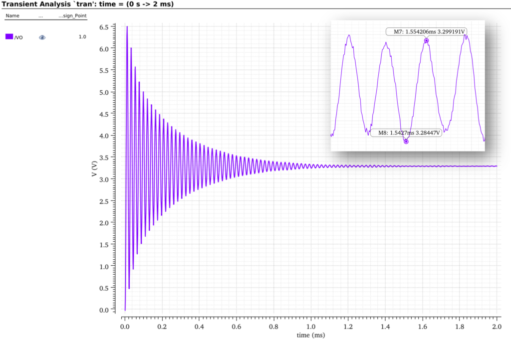
- Validated through Cadence ADE simulations: VGS drive signals, level shifter operation, bootstrap functionality; achieved 5.15% output ripple and 198 mA inductor current ripple.
- Design targets: Vin=12 V, Vout=3.3 V, Iout=1 A, fsw=2 MHz. Implemented synchronous buck topology with MOSFETs replacing diodes for freewheeling current.
- MOSFET sizing (TSMC 180 nm): Length fixed at 900 nm per PDK models. Widths optimized via parametric sweeps-High-side ≈ 65.6 mm, Low-side ≈ 96.4 mm-minimizing total loss under a 1 A load.
- Gate driver architecture:
- Up-/down-level shifters for voltage translation.
- Bootstrap circuit for high-side drive.
- Dead-time generator to suppress shoot-through.
- Final driver stage tuned: HS rise 5 ns, LS rise 2 ns, fall 1 ns.
- Validation results: Verified PWM input propagation, VGS(HS/LS) waveforms, level-shifter I/O integrity, bootstrap charging. Measured 5.15% output ripple and 198 mA inductor ripple, confirming spec compliance.
Two-Stage CMOS Op-Amp
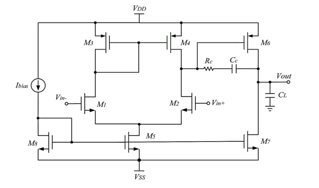
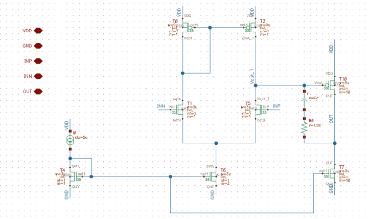
- Designed and implemented a two-stage CMOS op-amp in IBM 130 nm technology (single 1.5 V supply, CL=2 pF).
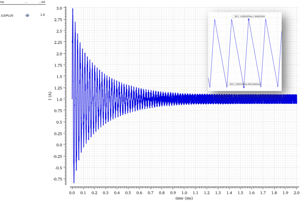
- Validated via multiple testbenches: gain/GBW/PM, slew rate, output swing, and CMRR; ensured all devices remained in saturation.
- Achieved 83 dB gain, 13.5 MHz GBW, 60° phase margin, and 94 µW power using a small-signal-driven sizing flow (gm/ID≈11.5 S/A).
- Targets & model: UGF=10 MHz, PM ≥ 60°, CL=2 pF, VDD=1.5 V; classical two-stage Miller-compensated op-amp.
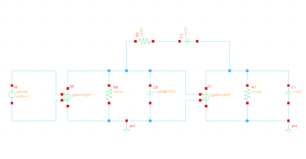
- Compensation: CC=1.3 pF (increased from 1.0 pF to meet PM), RC≈1/gm6 ≈ 1.8 kΩ.
- Biasing: Ibias=5 µA, IM5=10 µA; ~50 µA through the second stage (slew-rate constraint).
- Final sizing (W/L in µm/µm): M1,2=3/1.2, M3,4=9/1.2, M5=6/1.2, M6=90/1.2, M7=30/1.2, M8=3/1.2; gm/ID≈11.5 S/A.
- Results (sim): Avd=83.31 dB, OVSR=1.2426 V, SR=6.87 V/µs (avg), CMRR=81.5 dB, GBW=13.55 MHz, PM=60.34°, Pdiss=94.17 µW.
- Spec constraints: Single ideal current source; all specs (Avd, SR, CMRR, GBW, PM, Pdiss) met or exceeded.
PCB Design of hybrid DC DC Converter
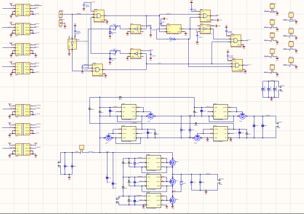
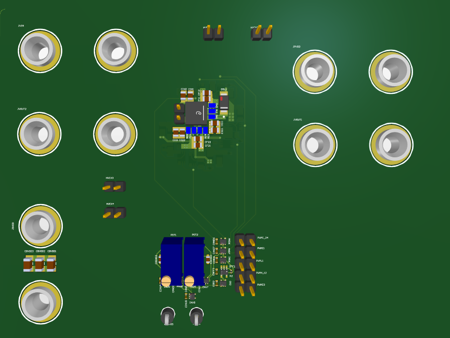
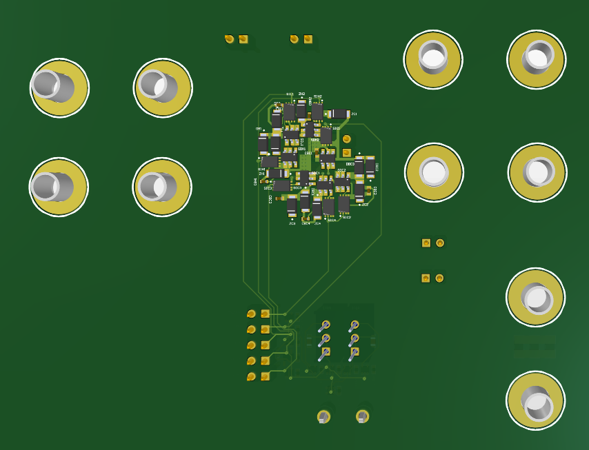
- Designed a four-layer hybrid-converter PCB in Altium Designer from scratch, including custom schematic/footprint libraries, organized project structure, and final manufacturing outputs (Gerber + drill files).
- Top/Bottom carefully partitioned for the power stage and control signals; internal planes dedicated to GND and VDD to provide low-impedance returns and clean supply distribution.
- Separated power and control paths, minimized switching-loop area and return path length, and placed decoupling with solid plane referencing to reduce EMI.
ECG Based Biometric Recognition
Open Project
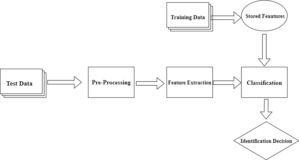
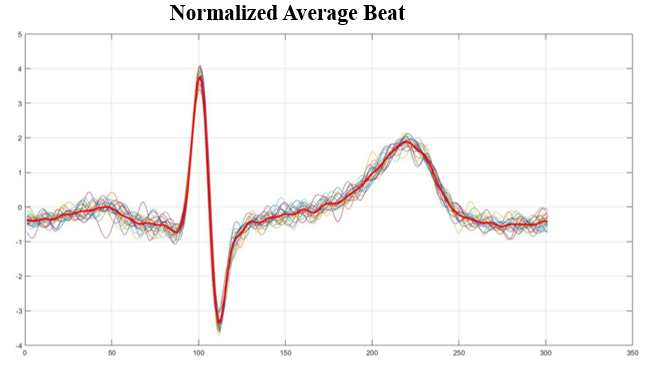
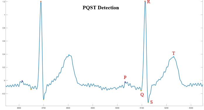
- Designed a biometric recognition system to authenticate individuals using ECG signals.
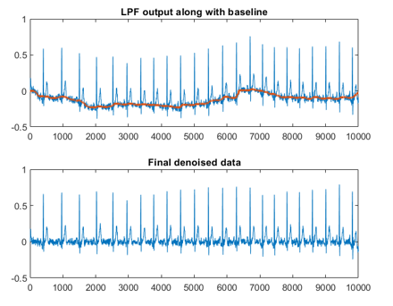
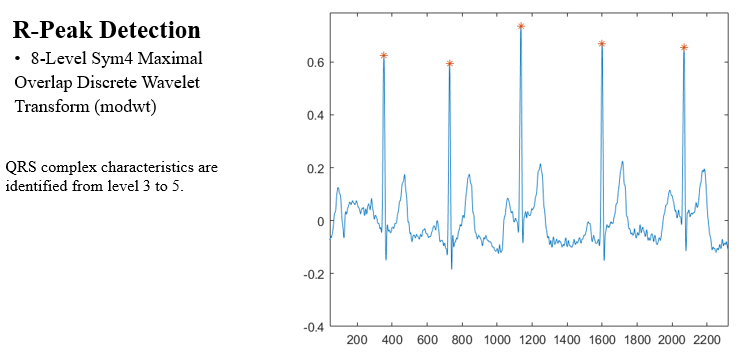
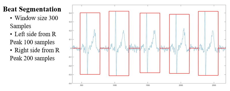
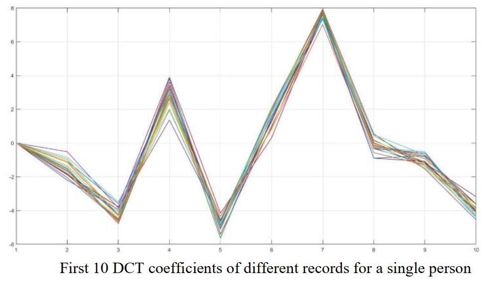
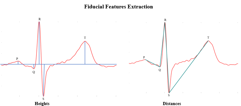
- Applied advanced signal processing techniques, including Chebyshev low-pass filters, median filters, and Maximal Overlap Discrete Wavelet Transform for feature extraction.
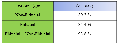
- Utilized the Weighted K-Nearest Neighbors algorithm with the Euclidean distance method for classification, validated through a 5-fold cross-validation process.
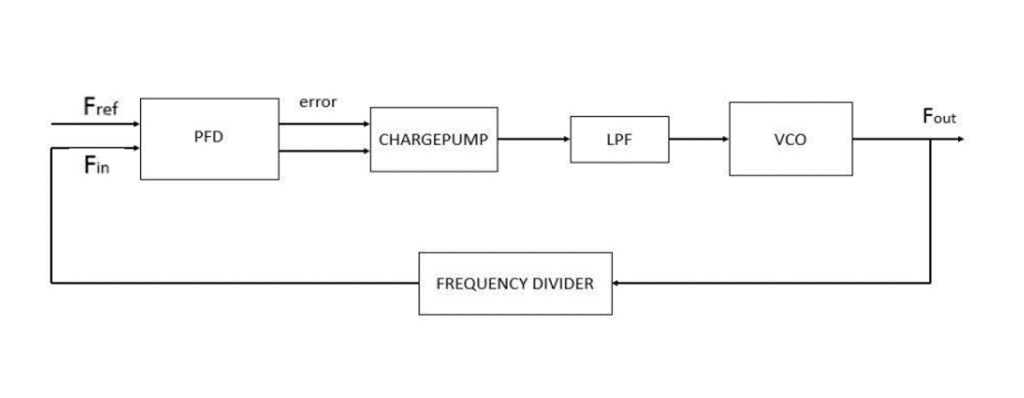
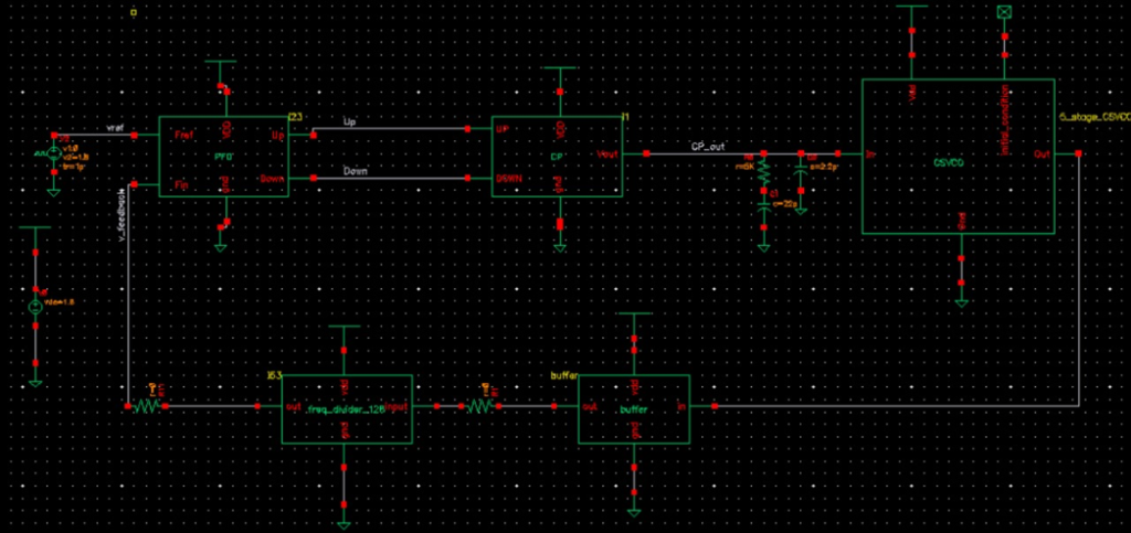
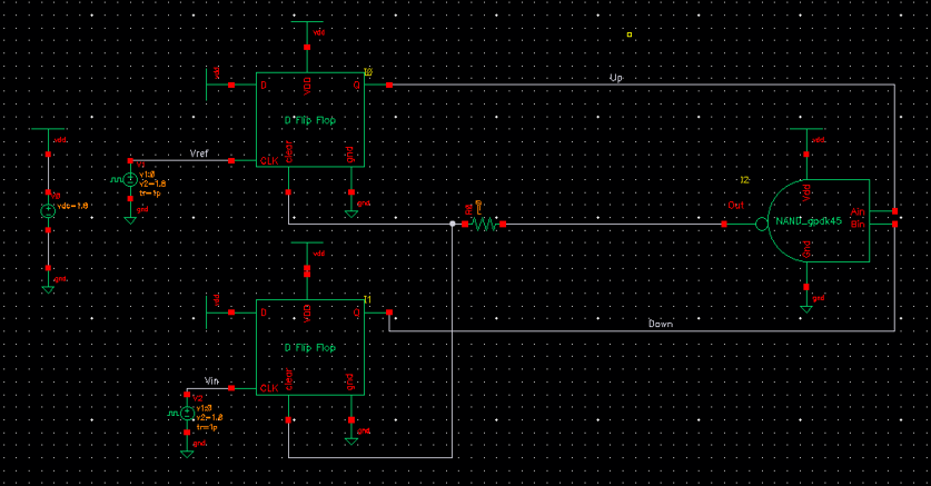
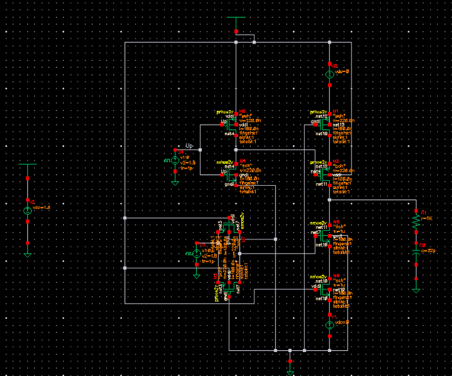
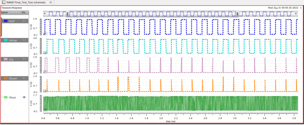
Phase-Locked Loop : Design & Implementation
Open Project

